
ADI AD9122高速DAC和ADL5373 I-Q調制器接口解決方案
發布時間:2011-8-29 12:10
發布者:Liming
|
ADI公司的AD9122是雙路高動態范圍的高速DAC,取樣速率1230MSPS,靈活的LVDS接口, 122.88 MHz IF的單載波WCDMA ACLR為82dBc, RL = 25 Ω to 50 Ω時的模擬輸出從8.7 mA 到31.7 mA可調,集成了2x/4x/8x內插/復數調制器,使得載波可放置在DAC帶寬內任何地方, 1.2 GSPS的功率為1.5W, 500 MSPS的功耗為800mW,主要用在無線基礎設備, W-CDMA, CDMA2000, TD-SCDMA, WiMAX, GSM, LTE和寬帶通信如LMDS/MMDS,點對點通信,數字高或低IF合成.本文介紹了AD9122主要特性, 功能方框圖, AD9122評估板以及AD9122高速DAC和ADL5373 I-Q調制器接口解決方案,包括接口電路, AD9122-M5375-EBZ評估板電路圖和材料清單. Interfacing the ADL5375 I/Q Modulator to the AD9122 Dual Channel, 1.2 GSPS High Speed DAC The AD9122 is a dual, 16-bit, high dynamic range digital-to- analog converter (DAC) that provides a sample rate of 1230 MSPS, permitting multicarrier generation up to the Nyquist frequency. The AD9122 TxDAC+® includes features optimized for direct conversion transmit applications, including complex digital mod- ulation, and gain and offset compensation. The DAC outputs are optimized to interface seamlessly with analog quadrature modulators, such as the ADL537x F-MOD series from Analog Devices, Inc. A 4-wire serial port interface provides for program- ming/readback of many internal parameters. Full-scale output current can be programmed over a range of 8.7 mA to 31.7 mA. The AD9122 comes in a 72-lead LFCSP. PRODUCT HIGHLIGHTS 1. Ultralow noise and intermodulation distortion (IMD) enable high quality synthesis of wideband signals from baseband to high intermediate frequencies (IF). 2. Proprietary DAC output switching technique enhances dynamic performance. 3. Current outputs are easily configured for various single- ended or differential circuit topologies. 4. Flexible LVDS digital interface allows the standard 32-wire bus to be reduced to one-half or one-quarter of the width. AD9122主要特性: Flexible LVDS interface allows word, byte, or nibble load Single-carrier W-CDMA ACLR = 82 dBc at 122.88 MHz IF Analog output: adjustable 8.7 mA to 31.7 mA, RL = 25 Ω to 50 Ω Integrated 2×/4×/8× interpolator/complex modulator allows carrier placement anywhere in the DAC bandwidth Gain, dc offset, and phase adjustment for sideband suppression Multiple chip synchronization interfaces High performance, low noise PLL clock multiplier Digital inverse sinc filter Low power: 1.5 W at 1.2 GSPS, 800 mW at 500 MSPS, full operating conditions 72-lead, exposed paddle LFCSP AD9122應用: Wireless infrastructure W-CDMA, CDMA2000, TD-SCDMA, WiMAX, GSM, LTE Digital high or low IF synthesis Transmit diversity Wideband communications: LMDS/MMDS, point-to-point 
圖1.AD9122功能方框圖
圖2.AD9122典型的信號鏈框圖 AD9122評估板 The AD9122 Evaluation Board connects to the Analog Devices Digital Pattern Generator (DPG2) to allow for quick evaluation of the AD9122. The DPG2 allows the user to create many types of digital vectors and transmit these at speed to the AD9122 in any of the AD9122 operating modes. The AD9122 evaluation board is configured over USB with accompanying PC software.
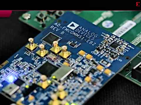
圖3. DPG2和AD9122評估板外形圖
圖4.AD9122評估板和DPG2連接圖 AD9122高速DAC和ADL5373 I-Q調制器接口解決方案 This circuit provides a simple and flexible interface between the AD9122 dual high speed TxDAC digital-to-analog converter and the ADL5375-05 broadband I/Q modulator.Because the DAC outputs and ADL5375-05 I/Q modulator inputs share a common bias level of 0.5 V, there is no need for any active or passive level shifting circuitry. The dc coupled interface facilitates I/Q modulator local oscillator (LO) leakage compensation by the DAC. The 1.2 GSPS AD9122 DAC sampling rate and the wide bandwidth of the ADL5375-05 modulator I and Q inputs ensure that both zero-IF (ZIF) or complex-IF (CIF) architectures can be supported. In addition to filtering Nyquist images, the baseband filter provides excellent rejection of both differential-mode and common-mode DAC spurs.
圖5.AD9122和ADL5375-50接口電路: 50 Ω電阻接地, 500 mV DC偏壓用于ADL5375-50帶通濾波器輸入
圖6.AD9122和ADL5375-50接口電路:10MHz三階Bessel濾波器
圖7.推薦的AD9122和ADL5375-50接口電路:Fc=300MHz五階Butterworth濾波器
圖8.AD9122-M5375-EBZ評估板外形圖
圖9.AD9122-M5375-EBZ功能測試連接圖
圖10. AD9122-M5375-EBZ電路圖(1)
圖11. AD9122-M5375-EBZ電路圖(2)
圖12. AD9122-M5375-EBZ電路圖(3)
圖13. AD9122-M5375-EBZ電路圖(4)
圖14. AD9122-M5375-EBZ電路圖(5)
圖15. AD9122-M5375-EBZ電路圖(6) AD9122-M5375-EBZ材料清單見:  AD9122-M5375-EBZ材料清單.rar
(7.62 KB)
AD9122-M5375-EBZ材料清單.rar
(7.62 KB)
http://www.analog.com/static/imported-files/data_sheets/AD9122.pdf 和 http://www.analog.com/static/imported-files/circuit_notes/CN0205.pdf |


網友評論